?2024年11月18-21日,第十屆國際第三代半導體論壇(IFWS2024)&第二十一屆中國國際半導體照明論壇(SSLCHINA2024)、先進半導體技術應用創新展(CASTAS)將在蘇州國際博覽中心G館舉辦。
乾晶半導體有限公司將亮相此次展會。誠摯邀請第三代半導體產業同仁共聚論壇,蒞臨C02號展位參觀交流、洽談合作。深圳市匯芯通信技術有限公司、國家5G中高頻器件創新中心副總經理、CTO許明偉將出席論壇,并在“氮化鎵射頻電子器件與應用分會”上帶來“FLAB:特色射頻半導體的技術創新模式探索”的的主題報告,敬請關注!
公司簡介
乾晶半導體有限公司2020年7月成立于浙江大學杭州國際科創中心,專注于第三代半導體材料領域,是一家集半導體碳化硅單晶生長、晶片加工和設備開發為一體的高新技術企業。公司的核心團隊來自于浙江大學硅材料國家重點實驗室,與浙大科創中心先進半導體研究院成立聯合實驗室共同承擔SiC材料的產業化任務,力爭在三到五年內打造成為國際知名的第三代半導體材料品牌和標桿企業,為第三代半導體產業提供有力支撐。
IVSEMITEC CO., LTD.?was established in July 2020 at the Hangzhou International Science and Technology Innovation Center of Zhejiang University (ZJU-HIC). It focuses on the field of third-generation semiconductor materials and is a high-tech enterprise that integrates semiconductor silicon carbide single crystal growth, wafer?processing, and equipment development. The core team of the company comes from the State Key Laboratory of Silicon Materials of Zhejiang University. It has established a joint laboratory with the Advanced Semiconductor Research Institute of ZJU-HIC to jointly undertake the industrialization task of SiC materials, and strives to become an internationally well-known brand and benchmark enterprise of third-generation semiconductor materials within three to five years, providing strong support for the third-generation semiconductor industry.?

產品簡介
6英寸導電型4H-SiC襯底
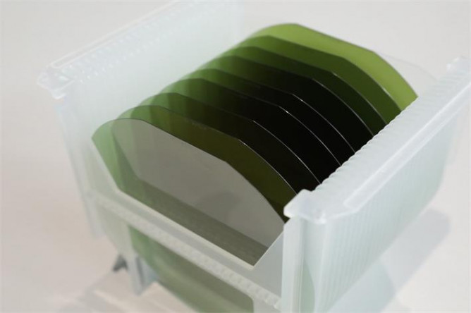
直徑:(150 ± 0.2) mm
厚度:(350 ± 25) μm
導電類型:n-type
晶面取向:(0001) 向 [11-2 0]偏4度
微管密度:≤0.1?/cm2
位錯密度:TSD≤100/cm2?;?BPD≤500/cm2
應用方向:SiC?SBD 或者SiC?MOSFET
產品類型:拋光片(Epi-ready)
8英寸導電型4H-SiC襯底
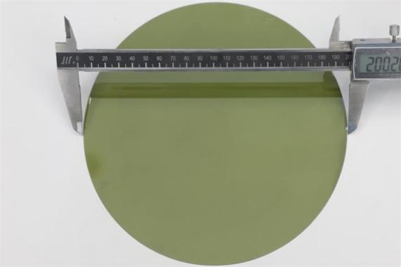
直徑:(200.0± 0.2) mm
厚度:(500 ± 25) μm
導電類型:n-type
晶面取向:(0001) 向 [11-2 0]偏4度
微管密度:≤0.2?/cm2
位錯密度:TSD≤300/cm2?; BPD≤1000/cm2
應用方向:SiC SBD 或者SiC MOSFET
產品類型:拋光片(Epi-ready)
?6英寸導電型碳化硅晶錠
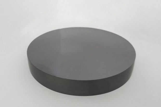
直徑:(150 ± 0.25) mm
厚度:10~20mm
導電類型:n-type
晶面取向:(0001) 向 [11-2 0]偏4度
產品類型:晶錠
8英寸導電型碳化硅晶錠

直徑:(200.0± 0.2) mm
厚度:10 ~ 20 mm
導電類型:n-type
晶面取向:(0001) 向 [11-2 0]偏4度
產品類型:晶錠
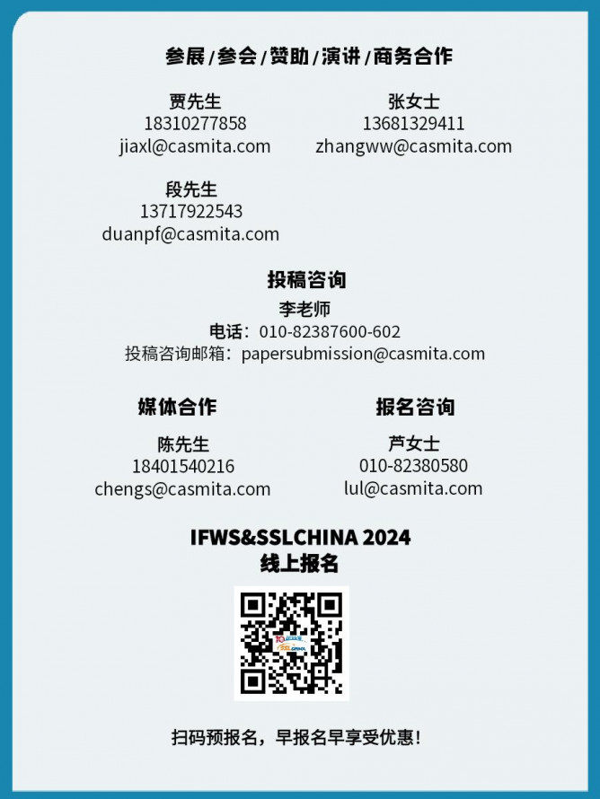
參會聯系
?